AI Chip News:
The most frequently mentioned companies are:
Nvidia.
TSMC.
Samsung.
SK Hynix.
But if you look further upstream:
You'll encounter a very unique company.
ASML.
It is not:
An AI model company.
Nor is it:
A chip design company.
Or even:
A foundry that actually manufactures chips for customers.
What it sells are:
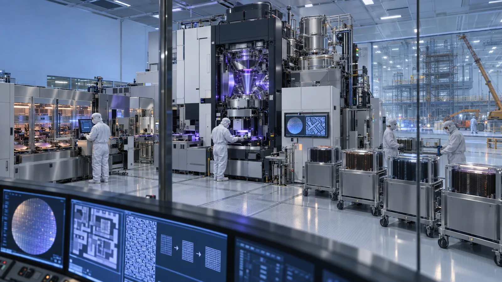
Machines that "print" chip circuits onto silicon wafers.
And as AI chips move toward more advanced processes:
These machines:
Becomes increasingly irreplaceable.
Reuters Reports a Stunning Figure Today
ASML’s most advanced mass-production EUV equipment costs roughly:
$200 million per machine.
Despite this high price:
Current orders are nearly filled through:
2027.
Next up is:
The next-generation High-NA EUV.
Priced even higher, about:
$400 million each.
Yet leading chipmakers have started lining up.
TSMC, Samsung, SK Hynix Set High-NA Timelines
Reuters reports today that:
Samsung plans to use High-NA in memory production from:
2028.
SK Hynix has similar plans for:
2028.
TSMC, which initially expressed doubts about High-NA’s staggering $400 million price tag, has committed to introducing it from roughly:
2030.
Intel is moving even faster.
Intel Has Already Processed Over One Million Wafers Using High-NA
Intel is among the earliest customers to conduct large-scale testing of High-NA.
ASML announced in July that Intel Foundry employed High-NA on certain layers of its Intel 18A process.
Reuters further reports Intel’s use of High-NA systems has already processed more than:
1 million wafers.
This is significant not because of the number itself, but because High-NA is no longer just a lab demonstration.
What Exactly Is EUV?
Chip manufacturing can be roughly understood as:
Drawing extremely tiny circuits onto a small silicon wafer.
The smaller the circuits:
The more transistors you can fit into the same area.
This generally means:
Higher performance,
Lower power consumption,
Or the ability to build smaller chips with equal performance.
The problem is:
The circuits on chips are so small that conventional optical methods can no longer draw them.
EUV Addresses This Challenge
EUV stands for:
Extreme Ultraviolet.
It uses:
Light with an ultra-short wavelength.
Paired with extremely precise:
Mirrors,
Vacuum environments,
Stages,
and optical control systems.
This projects ultra-fine circuit patterns onto wafers.
EUV is among the most challenging equipment in advanced chip manufacturing.
Why Is Everyone Talking About ASML?
Because in the most advanced EUV market segment, commercially:
ASML holds almost the entire share.
JPMorgan estimates that in 2025, ASML will control about:
94% of the global lithography market.
Its dominance in advanced EUV is even greater.
Reuters directly states:
ASML currently has no commercial EUV competitors.
Why Not Nikon, Canon, or Chinese Equipment Makers?
Japanese companies Nikon and Canon, as well as emerging Chinese equipment firms, produce lithography technologies such as DUV.
But EUV is far more difficult.
It’s not just about “making the light shorter.”
EUV Cannot Use Conventional Lenses
Because EUV light is readily absorbed by materials, traditional lenses are unsuitable.
ASML must rely on:
Ultra-precise mirrors
operating inside a vacuum environment to control the light.
ASML describes these mirrors as having surface flatness finer than the thickness of a single atom.
To put it in perspective, if the mirror were enlarged to the size of Germany, the tallest “peak” on its surface would be about:
1 mm.
This is no ordinary mechanical equipment.
High-NA Advances Beyond Current EUV
The current mainstream EUV has a numerical aperture (NA) of about:
0.33.
High-NA increases this to:
0.55.
NA roughly measures how finely an optical system can resolve patterns.
As NA increases, smaller features can be printed.
ASML claims EXE High-NA enables about:
8 nm resolution.
High-NA Prints Features About 1.7 Times Smaller in a Single Exposure
Compared to current NXE EUV:
High-NA can print features about:
1.7 times smaller in a single exposure.
Theoretically, transistor density can increase by approximately:
2.9 times.
Reuters puts it simply:
High-NA allows for printing features roughly:
40% smaller than standard EUV.
Why Is a 40% Feature Size Reduction So Important?
Chip manufacturing isn’t just about hitting the smallest nanometer size.
More important is whether a pattern can be done in a single exposure.
If a machine’s resolution isn’t enough, you may have to split what could be a one-step pattern into:
Two,
Three,
Or even more steps.
This is called multi-patterning.
Multi-Patterning Increases Cost With Each Additional Step
More exposures.
More etching.
More cleaning.
More alignment.
More process steps.
All of which means:
More time,
More equipment use,
More materials,
And higher risks to yield.
So even if the High-NA machine itself is very expensive, if it can convert layers that previously required multiple patterning into single exposure, overall costs can be valuable.
This Explains Why Price Alone Isn’t the Whole Story
Even if a machine costs $400 million, that might seem outrageous.
But for an advanced foundry producing high-value AI chips in large volumes:
The key metrics are:
How many wafers per time?
What is the yield?
How many process steps are needed?
Equipment downtime?
Ultimately, what is the cost per good chip?
So foundries really compare:
Cost per good wafer,
not the sticker price of the equipment.
High-NA Also Reduces Process Complexity
ASML states that with improved resolution, High-NA enables some processes to revert from multi-patterning to single patterning.
This reduces production cycle time and simultaneously increases wafer output.
This is the real reason customers consider investing in a $400 million machine.
Why Did TSMC Have Doubts Previously?
Because semiconductor performance can be enhanced not only by shrinking transistor sizes.
Other approaches include:
Advanced packaging,
Chiplets,
3D stacking,
HBM,
which combine chips more efficiently.
The industry previously questioned:
Is it really necessary to adopt High-NA so soon?
Or can packaging extend the performance improvements more cost-effectively?
The Biggest Signal Today: Major Manufacturers Are Now Committing to High-NA
TSMC, Samsung, SK Hynix, Intel, and Micron have either purchased, committed to, or scheduled High-NA integration plans.
This indicates these large chipmakers believe:
Advanced process scaling is not over yet.
Packaging and High-NA will continue in parallel.
It’s not an either/or choice.
High-NA Is Especially Critical for AI Since AI Chips Demand Everything
AI accelerators need:
More compute power,
Higher memory bandwidth,
Lower power consumption,
Faster interconnects,
More transistors.
Thus, GPUs, ASICs, HBM, networking, advanced packaging, and foundries all push forward together.
Among these, lithography is the foundational key enabling actual chip manufacturing.
Designing a Larger GPU Doesn’t Mean Nvidia Can Manufacture It Alone
Nvidia excels at:
Architecture,
CUDA,
Software ecosystem,
and chip design.
But turning designs into silicon requires:
TSMC,
which in turn relies on numerous equipment suppliers.
In advanced lithography, ASML occupies a uniquely critical position.
So the AI chip supply chain is not just about one company, Nvidia.
AI Is Actually a Long Physical Chain When Viewed from Models Down
At the top:
ChatGPT,
Claude,
Gemini.
Below that:
Model training.
Further down:
GPU, ASIC.
Then:
HBM, advanced packaging, wafers, foundries, lithography, chemicals, materials, electricity.
This shows that software-based AI rests on a huge physical infrastructure.
ASML’s Unique Power: Competitors in Chips All Rely on It
TSMC and Samsung compete as foundries.
Samsung and SK Hynix compete in memory.
Intel aims to reclaim advanced process leadership.
Micron seeks to expand memory production.
They are fierce competitors, but in lithography, they all become ASML’s customers.
This is a very rare position.
Reuters: ASML’s Existing EUV Orders Are Almost Sold Out Through 2027
AI demand is driving advanced chip capacity rapidly.
ASML CFO Roger Dassen describes recent talks with a major customer as basically asking:
Can you give us more?
Can it come faster?
This reflects customer concerns are no longer about “is there demand?” but rather “when will equipment arrive?”
ASML Is Expanding Production
Reuters reports ASML recently broke ground in Eindhoven for a new large production base.
This region is expected to accommodate up to 20,000 employees for manufacturing, logistics, office work, and related facilities.
This is a clear signal that ASML bets on continued advanced semiconductor demand.
ASML CEO Says He Doesn’t Believe the AI Boom Has Ended
ASML CEO Christophe Fouquet told Reuters he does not think the AI boom is over.
Of course, this is a company leader’s perspective and not a guarantee AI growth will continue indefinitely.
But it reflects strong current customer demand.
High-NA Faces an Interesting New Problem: Photomasks Are Too Small
Chips are not directly written onto wafers by AI.
They require photomasks—templates that carry circuit patterns used by exposure machines.
The industry mainly uses 6-inch masks now.
But High-NA’s different optical design introduces new constraints on exposure area.
TSMC and ASML Collaborate to Develop 12-Inch Photomasks
On September 8, ASML and TSMC announced a new industry collaboration initiative to promote:
12-inch photomasks.
High-NA can still use current 6-inch masks initially and isn’t unusable without 12-inch masks.
Larger masks could improve scanner productivity, reduce some chipmaking costs, and ease stitching limitations for large chips.
Their Goal Extends to 2031 and 2033
ASML and TSMC’s plans include:
Establishing a 12-inch mask pilot line by 2031, and
Supporting full advanced-node production readiness by 2033.
This reminds us chip manufacturing decisions are made years in advance.
Chip Manufacturing Decisions Are Made Many Years Ahead
Conversations in 2026 are about 2030, 2031, and 2033.
This may seem distant, but redesigning exposure equipment, masks, materials, processes, fabs, inspection, and supply chains requires many years.
The real timeline for the AI chip race is much slower than rapid model updates.
Models May Change Every Three Months, But Foundries Can’t Be Rebuilt That Fast
This presents a big contradiction in AI:
Software evolves very fast,
Infrastructure evolves very slowly.
Model demand may suddenly double, but fabs, power plants, lithography machines, and HBM plants cannot be ordered today and delivered next week.
This explains ongoing bottlenecks in AI supply chains.
Today It May Be HBM, Tomorrow Electricity, The Day After Exposure Equipment
Recently we have seen shortages of:
HBM,
Data center electricity,
Transformer cooling,
Advanced packaging,
AI servers,
various bottlenecks appearing in rotation.
The fundamental issue is AI scale demands the entire supply chain to expand simultaneously, not just one resource.
High-NA Deserves Attention Because It’s the Hardest to Scale Quickly
More GPU designers can enter the market.
More AI models can be trained.
More cloud infrastructure can be built.
But when it comes to the most advanced EUV technology:
ASML alone holds the position.
Not because others are unwilling, but because of deep accumulated technology.
EUV Took Decades to Reach Its Current State
High-NA is not something ASML suddenly conceived this year and instantly completed.
Light sources, mirrors, optics, stages, vacuum, materials, masks, inspection, and metrology all need mature industrial chains.
This is the true technological moat and the hardest aspect to replicate.
It’s not a single patent but decades of integrated system know-how.
So Today’s Reuters Story Is Not Just About Selling Expensive Machines
The key takeaway is:
Where the industry once doubted whether High-NA would be widely adopted, major chipmakers are now increasingly committing to it.
Intel is already working with it.
Samsung and SK Hynix plan to ramp in 2028.
TSMC maps out 2030.
Micron has placed orders.
This means the next phase of advanced process scaling is crystallizing.
This Is Especially Important for Taiwan
Because TSMC is one of the world’s most important advanced foundries.
Nvidia, Apple, AMD, and large AI chip designers all depend heavily on TSMC for manufacturing.
So when TSMC adopts High-NA and balances costs, yields, packaging, and processes, it will indirectly impact global AI chip production.
But High-NA Does Not Mean AI Chips Cannot Be Made Without It
Many AI chips today still rely on existing EUV and even mature process nodes to accomplish various functions.
AI chip progress won’t stop before 2030.
Advanced packaging, chiplets, architectures, memory, and software optimization will also continue to evolve.
High-NA represents a very important roadmap but not the only path.
ASML’s EUV Monopoly Still Carries Risks
Equipment is very expensive.
Customers are highly concentrated.
The semiconductor industry is cyclical.
Export controls influence which markets can buy which equipment.
High-NA itself must prove its production economics justify the investment.
Technology leadership doesn’t guarantee all customers will switch quickly to new machines.
TSMC’s 2030 Adoption Reflects Its Cautious Approach
Foundries don’t buy the newest equipment just because it’s new.
They consider yield, cost, throughput, customer needs, and process integration.
If existing EUV plus improved packaging can meet demands cost-effectively, there’s less urgency to adopt High-NA early.
TSMC’s timeline is therefore quite reasonable.
Memory Manufacturers May Be More Aggressive
Reuters reports ASML’s CEO believes memory makers face a lower threshold to adopt High-NA.
One reason is memory chips are smaller in size.
Samsung and SK Hynix already include 2028 in their production plans.
This directly impacts AI:
The HBM needed by AI GPUs is currently one of the most scarce resources.
GPU, HBM, Foundry, Lithography Are All Part of the Same AI War
Nvidia needs stronger GPUs.
GPUs depend on TSMC.
AI accelerators require HBM.
HBM depends on Samsung, SK Hynix, and Micron.
Advanced logic and memory require more advanced manufacturing equipment.
And it all ties back to ASML.
No company can do everything alone.
That’s Why the AI Supply Chain “Moats” Matter More Than Model Rankings
Benchmarks and leaderboards change every month.
But lithography technology can take a decade or two to develop.
Building a fab takes years.
Establishing a full supplier ecosystem may take decades.
Asked what advantages in the AI boom are hardest to replicate quickly, ASML is a classic answer.
Ultimately, AI Depends Not Just on the Smartest Models
Success also depends on who controls:
Chips,
Memory,
Equipment,
Packaging,
Energy,
Fabs, and
Supply chains.
While everyone discusses GPT-6, Claude, Gemini, and the next generation of models, the real engines running those models might be a $400 million machine buried thousands of kilometers away inside a cleanroom, layer by layer printing circuits onto wafers.
Top global chipmakers, despite their competition, still queue for orders with this single equipment supplier.
This is the reality of the AI supply chain worth attention tonight.
Today, progress with AI a little every day.
Learn one AI trick daily.
Save a little time daily.
Improve capabilities daily.
SasaDaily, growing with you.
Recommended Reading
Anthropic Designs Claude But Now Wants to Design AI Chips Too—Why?
When Chip Sellers Vouch for Chip Buyers, Is the AI Hype Entering a Dangerous Cycle?