Just yesterday, news surfaced that CXMT is preparing to enter the NAND market.
Today, it delivers an even more direct message:
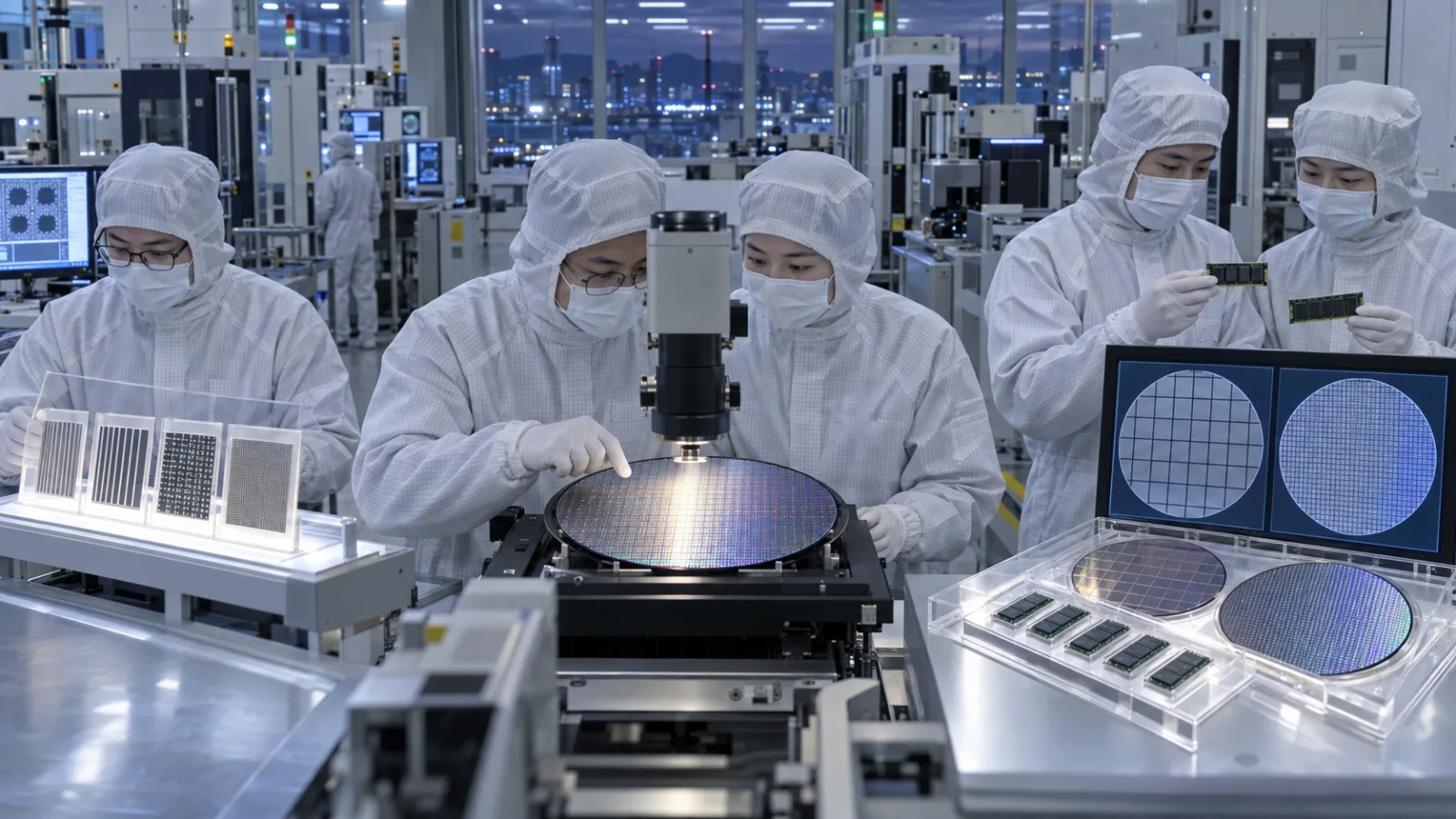
Its core DRAM manufacturing process has officially entered mass production.
Chinese memory manufacturer CXMT announced today that
its 5th-generation DRAM Technology Platform has now reached mass production.
There are three key numbers to note:
11.95nm
24Gb
and
at least a 50% increase in gross chip dies per wafer.
These numbers don’t mean just:
“They’ve released a new memory chip.”
Instead, it means:
The same silicon wafer can now house more, denser DRAM chips.
To clarify: This is not an HBM announcement
Seeing words like:
CXMT,
Memory,
AI,
it’s easy to think immediately about HBM (High Bandwidth Memory).
But today CXMT officially announced two products:
24-gigabit LPDDR5X.
LPDDR5X is mainly used in:
- Smartphones
- Tablets
- Portable electronics
It emphasizes low power consumption and high memory density.
This is not the kind of HBM next to Nvidia GPUs that provides ultra-high bandwidth specifically for AI accelerators.
Therefore, this article should not say:
“China officially mass-produces next-gen AI HBM.”
That would be inaccurate.
The true breakthrough today is a more fundamental one:
DRAM process capability.
What exactly is DRAM?
You can think of computer memory as a work desk.
SSD/NAND is more like a:
filing cabinet.
Data is stored there long-term.
DRAM, on the other hand, is like the:
desktop you’re currently working on.
When a CPU, phone processor, or server runs programs,
it relies on DRAM for fast access to large amounts of temporary data.
So from:
smartphones,
PCs,
cloud servers,
to data centers,
and AI workloads,
DRAM is indispensable.
At the very top tier in AI accelerators,
even faster and specially packaged memory called:
HBM
is also used.
How small is 11.95nm?
CXMT said today that
its 5th-generation platform shrinks the key spacing between memory cells to:
11.95 nanometers.
That is approximately:
12 billionths of a meter.
Simply put:
Previously on a wafer,
each storage cell required larger space.
Now, with reduced spacing,
the same area can fit:
more memory cells.
The outcome is:
more data stored on each chip,
and more chips potentially produced per wafer.
This is one of the core goals of memory process advancement.
Without cutting-edge EUV lithography, how does CXMT continue shrinking?
This is where today’s most interesting technology appears:
Quadruple Patterning.
In Chinese, this translates to:
fourfold patterning.
Don’t worry about the semiconductor jargon for now.
Think of it this way:
If you originally use just one printing mask,
and it can’t print lines that fine in one pass,
then you:
first print a larger pattern,
then split it multiple times,
re-deposit material,
and etch repeatedly,
gradually transforming a thicker line into multiple finer lines.
In other words:
using more manufacturing steps to achieve finer circuitry.
This does come at a cost.
More steps typically mean:
more complex processes,
longer production time,
and more challenging error control.
But for China’s chip industry, limited by advanced lithography equipment,
this is a very practical path forward.
Why is this related to US export restrictions?
Since 2022,
the US has continuously restricted China’s access to certain:
advanced semiconductor equipment
and related software.
China’s chipmakers face the challenge:
If they can’t obtain the world’s most advanced equipment,
can they still use existing equipment plus process innovations to further shrink circuitry?
One answer CXMT demonstrates today is:
multi-patterning.
The company also says the platform development involved:
computer simulations,
and cooperation with local Chinese chip equipment makers for key steps.
So what’s truly worth watching isn’t just CXMT itself.
It’s that:
China is striving to localize “equipment + process + memory design” all at once.
New LPDDR5X chips pack 24Gb each
CXMT simultaneously introduced two:
24-gigabit LPDDR5X products.
Note: The Gb here stands for Gigabit,
not the 24GB often seen in smartphone advertising.
Since 8 bits = 1 byte,
24Gb equals approximately:
3GB per chip.
Phone makers can combine multiple memory dies or packages as needed to create
larger total memory capacities.
CXMT states that these two products offer a:
50% capacity increase
compared to their previous generation equivalents,
and are already in mass production.
This means it’s neither a:
research demo,
nor a laboratory prototype,
but ready to be part of the supply chain.
The bigger number is “50% more chips per wafer”
CXMT also says that using an 8Gb chip as a benchmark,
the 5th-generation platform enables at least a:
50% increase in gross chip dies per wafer
compared to the 4th generation.
This is an important figure.
Because chip costs aren’t just about:
how advanced each chip is,
but also:
how many chips can be cut from a single wafer.
Given the same 300mm wafer size,
if more chips can be sliced out,
the average manufacturing cost per die theoretically can decrease.
But there is an important caveat.
50% more gross dies doesn’t mean 50% more sellable chips
Reuters specifically reminds that:
CXMT cited:
Gross die count,
which means the theoretical number of chip dies from a wafer.
It’s not:
Yield.
Yield refers to the percentage of chips that pass testing and are ship-ready.
For example:
An old process wafer might have 500 chips with a 90% yield,
giving 450 usable chips.
A new process might have 750 chips, but if the early yield is 70%,
only 525 chips are usable.
The actual production increase is therefore less than the 50% increase in gross dies.
So:
A higher die count is promising,
but what truly determines cost competitiveness is:
whether yield can keep pace.
CXMT has not disclosed full yield data yet.
CXMT claims to have caught up with advanced mass production nodes
At the 2026 World Manufacturing Convention held in Hefei, CXMT’s Vice President Luo Xiaodong said:
the company’s process capability now compares to the industry’s most advanced mass production nodes.
This is CXMT’s own statement.
Reuters' report does not include independent verification from Samsung, SK Hynix, or Micron on this technology claim.
Thus, a more accurate way to phrase it is:
CXMT believes it has approached the most advanced mass-produced DRAM processes.
Instead of definitively stating:
China’s DRAM has fully caught up with Samsung and SK Hynix.
Market ranking gaps remain
CXMT is indeed progressing rapidly.
Reuters, summarizing data in July 2026, placed CXMT’s global DRAM market share at approximately:
7.7%
ranking it 4th worldwide.
Ahead of it remain the three traditional memory giants:
- Samsung
- SK Hynix
- Micron
So today’s mass production milestone truly means:
The 4th place player is narrowing the technology gap.
It does not mean the global rankings have changed overnight.
Why this still matters for AI
Because the AI boom isn’t just about GPUs.
AI workloads running in data centers
also require large amounts of:
- server DRAM
- HBM
- NAND storage
- networking
- power supplies
- cooling solutions
Reuters reported in June 2026 that CXMT and Tencent signed a long-term DRAM supply agreement worth over:
20 billion RMB
These DRAM chips will be integrated into Tencent’s servers,
which play a foundational role for cloud, databases, and AI workloads.
Therefore, CXMT is not focused solely on mobile memory.
The HBM line is also progressing
At the end of August, rumors surfaced that:
CXMT had started small-volume production of
HBM3E.
HBM3E is the advanced high-bandwidth memory used directly in high-performance AI chipsets.
Reports indicated that Chinese chip designers such as Alibaba T-Head and Cambricon are testing these chips.
However, that information came from The Information and was relayed by Reuters,
and it involved:
small-volume production
not today’s official announcement of
mass production.
So the evidentiary strength differs.
Today, CXMT formally confirms mass production of:
its 5th-generation DRAM platform and 24Gb LPDDR5X.
Yesterday’s NAND news is a separate track
Even more interestingly,
just two days ago Reuters exclusively reported that
CXMT is preparing to enter:
NAND flash.
The company reportedly plans to establish a:
NAND R&D production line at a new Beijing factory.
NAND and DRAM serve different functions.
DRAM:
temporarily stores active working data.
NAND:
stores data long-term.
AI servers now demand both in large quantities.
So, combining recent developments shows:
DRAM
5th-generation platform is mass produced today.
HBM
Reported small-volume production and customer validation of HBM3E.
NAND
Preparations underway for R&D production line setup.
This is the real picture worth noting today.
CXMT aims for more than just selling another mobile memory chip
If it were only today’s LPDDR5X,
the main market would remain mobile and portable devices.
But looking at
server DRAM,
HBM,
and NAND
together,
CXMT is gradually evolving from a
Chinese DRAM manufacturer
into a
more comprehensive memory supplier.
The AI boom is turning memory into a strategic asset again.
Because as computing power increases,
no matter how fast GPUs get,
if:
memory bandwidth is insufficient,
or server DRAM is lacking,
or storage is limited,
the entire system will bottleneck.
This is not an immediate threat to Samsung, SK Hynix, and Micron
Nor should this be interpreted as
Samsung, SK Hynix, and Micron being overtaken by CXMT tomorrow.
The biggest remaining gaps include:
- advanced process yield
- HBM scale
- advanced packaging
- global customer qualification
- production stability
- equipment access
These cannot be overcome by launching a new platform alone.
But the direction of competition is now clearer.
Previously, the biggest question for China’s memory supply chain was:
Does it exist?
Going forward, the battle will be about:
Can it mass produce?
And next will be:
yield, cost, capacity, and whether customers truly adopt at scale.
Today’s real turning point is shifting “can make” to “can mass produce”
Making a memory chip in a lab
and producing hundreds of thousands or millions daily in a factory
are completely different challenges.
The true difficulty in semiconductors is not:
making it for the first time.
It’s:
repeating the same pattern tens of thousands of times every day,
while maintaining:
consistent dimensions,
low defect rates,
low costs,
and high yields.
So the most important words from CXMT today aren’t:
“11.95nm.”
but:
“Mass Production.”
Only by crossing this line
does technology start truly impacting:
price,
supply,
customer choice,
and the global memory market.
The AI compute battle won’t be decided solely by who can build the fastest GPUs.
Large-scale AI systems require an entire supply chain of:
compute
+ memory
+ storage
+ network
+ power.
What CXMT crossed today brings the “memory” segment a step closer
to large-scale competition.
Today, advancing a little with AI.
Learning a new AI skill each day.
Saving a bit of time daily.
Improving a bit every day.
SasaDaily, growing with you.